Magnetron Sputtering Target
- Categories:Tungsten-molybdenum for Vapor Deposition
- Author:
- Origin:
- Time of issue:2017-11-21 00:00
- Views:
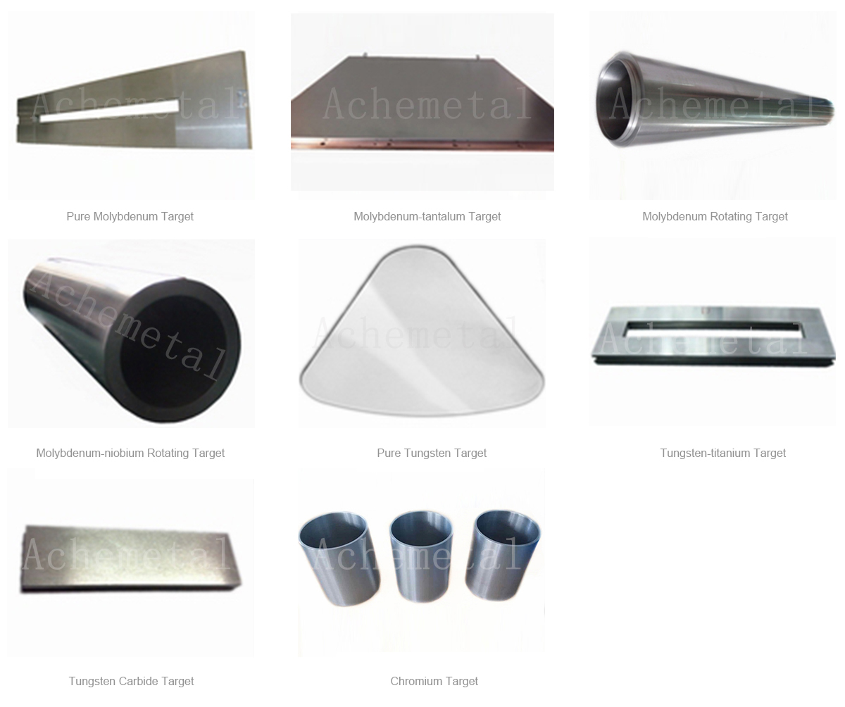
(Summary description)Sputtering is an advanced film material preparation technology. By the technology, ions generated by ion sources are gathered into high-speed ion flow at the accelerated speed in vacuum to impact solid surfaces, and ions are subjected to kinetic energy exchange with atoms on solid surfaces, so atoms on solid surfaces separate from targets and are deposited on the surfaces of substrates, thus forming nanometer (or micrometer) films. However, the impacted solids are raw materials deposited on the films by a sputtering method, which are called sputtering targets. Tungsten-molybdenum sputtering targets can form films on various substrates. The sputtering films are widely used as electronic parts and electronic products, such as TF-LCD (Thin Film Transitor-Liquid Crystal Displays), plasma display screens, inorganic LED displays, field emission displays, thin-film solar batteries, sensors, semiconductor devices as well as field effect transistor grids with tunable work function CMOS (complementary metal oxide semiconductor) and so on which are widely applied at present.
Magnetron Sputtering Target
(Summary description)Sputtering is an advanced film material preparation technology. By the technology, ions generated by ion sources are gathered into high-speed ion flow at the accelerated speed in vacuum to impact solid surfaces, and ions are subjected to kinetic energy exchange with atoms on solid surfaces, so atoms on solid surfaces separate from targets and are deposited on the surfaces of substrates, thus forming nanometer (or micrometer) films. However, the impacted solids are raw materials deposited on the films by a sputtering method, which are called sputtering targets. Tungsten-molybdenum sputtering targets can form films on various substrates. The sputtering films are widely used as electronic parts and electronic products, such as TF-LCD (Thin Film Transitor-Liquid Crystal Displays), plasma display screens, inorganic LED displays, field emission displays, thin-film solar batteries, sensors, semiconductor devices as well as field effect transistor grids with tunable work function CMOS (complementary metal oxide semiconductor) and so on which are widely applied at present.
- Categories:Tungsten-molybdenum for Vapor Deposition
- Author:
- Origin:
- Time of issue:2017-11-21 00:00
- Views:
Business Consulting:+86-13526941255 Yanyan
Email:yanyan@achemetal.net
Sputtering is an advanced film material preparation technology. By the technology, ions generated by ion sources are gathered into high-speed ion flow at the accelerated speed in vacuum to impact solid surfaces, and ions are subjected to kinetic energy exchange with atoms on solid surfaces, so atoms on solid surfaces separate from targets and are deposited on the surfaces of substrates, thus forming nanometer (or micrometer) films. However, the impacted solids are raw materials deposited on the films by a sputtering method, which are called sputtering targets. Tungsten-molybdenum sputtering targets can form films on various substrates. The sputtering films are widely used as electronic parts and electronic products, such as TF-LCD (Thin Film Transitor-Liquid Crystal Displays), plasma display screens, inorganic LED displays, field emission displays, thin-film solar batteries, sensors, semiconductor devices as well as field effect transistor grids with tunable work function CMOS (complementary metal oxide semiconductor) and so on which are widely applied at present.
Main factors of measuring the quality of targets include purity, density, grain size and its distribution, etc.
To ensure the quality of targets, Luoyang Achemetal adopts the following technologies:
a. Select high-purity molybdenum powder as a raw material;
b. By a fast densification formation sintering technology, the low porosity of targets can be ensured, and the grains size can be controlled;
c. The introduction of impurity elements is controlled strictly in the preparation process;
d. Apply a hot isostatic pressing method to parts of high-requirement products. Molybdenum-niobium targets prepared by this method are fine grain products with the extremely high density of 95%~99%.
In addition, Achemetal’s capacity of producing targets also has the following advantages:
1. Product enlargement: molybdenum alloy targets which have the single dimensions of 1,130mm *1,200mm *10mm and are suitable for G4.5 TFT coating equipment are produced;
2. Rotating targets with the length of more than 3m can be manufactured to meet the requirements of improving the utilization rate of targets in the market.
3. 10mm*200mm*L pure molybdenum targets of G8 wires or above can be produced.
4. High-quality metal and ceramic targets can be manufactured by hot isostatic pressing equipment.
 +8613526941255

 Message